Electronics and semiconductors

Metrology solutions for bulk and thin film-based electronic components manufacturing

The advancements in materials research and semiconductor technology have brought great changes to the way we live. They have driven developments in almost every aspect of our daily life – phones, smart wearables and toys, laptops, wireless networks, home infotainment systems, cars, and smart meters.

The electronic display, data storage, and RF filter technology industries have rapidly advanced, and the rate of change continues to follow Moore’s law. Growth technologies now allow the deposition of multilayered structures with individual layers exhibiting film thickness from microns down to monolayers.

Typical materials involved in advanced thin film devices are semiconductors, metal alloys, dielectrics, oxides, and polymers. This mandates accurate monitoring and control of the device parameters using multiple investigation techniques. Equally important is the fine control over the process materials, like CMP slurry, which is an indispensable part of any thin-film device manufacturing.

Frequently asked questions

Do I need to prepare the workspace prior to installation?
All instruments need a power source, and some have additional requirements such as a water supply or waste extraction. Where this the case, we will advise you prior to shipping your instrument.
What specialist skills or knowledge are required?
You don't need any specialist skills or knowledge to perform a Smart Install. Simply follow the instructions provided.
Do I need specialist tools or equipment to Smart Install a new instrument?
  • For installation of a Mastersizer or Zetasizer system, you will need a computer with internet access in order to view the installation guides. For installation of an Epsilon 1 XRF instrument, you will also need a smartphone or tablet to connect with our support personnel via a secure, augmented reality (AR) platform.
  • Everything else you need to install your new instrument will be provided.
What languages are available for the Smart Install guides?
  • Mastersizer: English, Chinese, Korean, French, German and Japanese
  • Zetasizer: English, Chinese, Korean, French, German and Japanese
  • Epsilon 1: English, French, German and Japanese, Spanish and Portuguese

Analytical solutions for the electronics industry

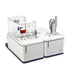
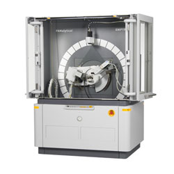
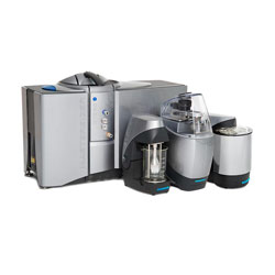
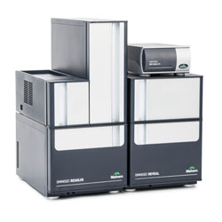
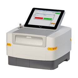
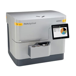
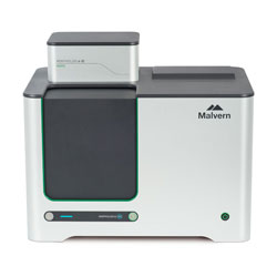
Malvern Panalytical is closely associated with the electronics industry with a wide range of solutions across the entire value chain:

  • XRF (2830 ZT) delivers thickness and composition information for a wide range of thin films, with contamination and dopant levels and surface uniformity on wafers up to 300mm in size.
  • XRD (X'Pert3 MRD and X'Pert3 MRD XL) provides absolute, calibration-free, and accurate information on crystal growth, giving material composition, film thickness, grading profile, and phase and crystal quality.
  • Laser diffraction (Mastersizer 3000) measures particle size distribution in powder and slurry dispersions, e.g. CMP slurry and electronic display materials.
  • Imaging (Morphologi 4) analyzes particle shape and morphology using automated imaging.
  • Zeta potential (Zetasizer Range) determines the stability of slurries used in the electronics industry through the measurement of zeta potential. It also measures particle size in nano-particle suspensions.
  • GPC/SEC (OMNISEC) analyses size, molecular weight, intrinsic viscosity, branching, and other parameters for polymers used in the electronics industry.
  • XRF (Epsilon 4): A chemical composition analysis of raw materials and finished products and RoHS/WEEE analysis of electronic components.
  • XRD (Aeris): A crystalline phase analysis of raw materials and finished products in electronics industry.

Our solutions

OMNISEC

GPC/SEC solution for the measurement of absolute molecular weight, intrinsic viscosity and other polymer parameters

OMNISEC

Aeris

Compact XRD to measure crystallite size and crystal phase

Aeris